Research facilities
A selection of the research facilities available in our group:
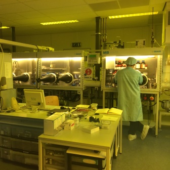
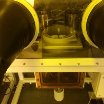
- A cleanroom class 7 with several glove boxes for spin coating, evaporators and preparation of solutions
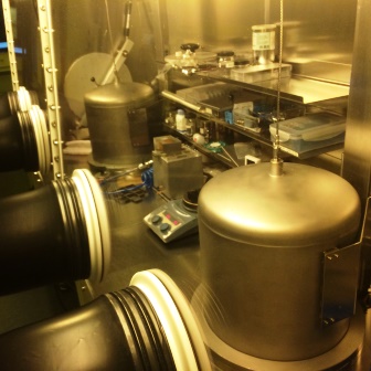
- Evaporators for deposition of thin layers of metals/compounds or organic materials
- Spin coaters outside (air environment) or inside glove box (N2 environment)
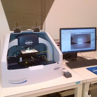
- Bruker Dektak XT profilometer to determine layer thickness and (large scale) roughness. Computer controlled XY table, vertical resolution down to nanometer scale, horizontal range μm - cm
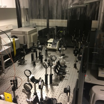
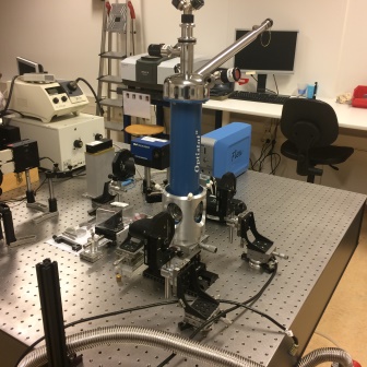
- Photoluminescence (PL) set-up: Titanium sapphire laser (Mira900) based femtosecond laser excitation. Steady state and time resolved (up to 1 ps resolution) measurements in the visible and NIR spectral range thanks to sets of Hamamatsu streak cameras and steady state detectors. The set-up is equipped with a second and third harmonic generator and it can be coupled to the confocal microscope.
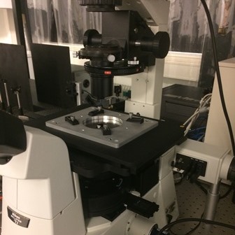
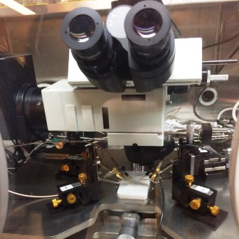
- Nikon Eclipse Ti confocal inverted microscope
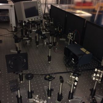
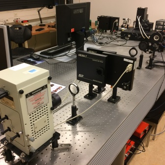
- Self-built transient absorption set-up based on a supercontinuum laser source and an auto-balanced photodetector. The laser covers a spectral range from 400 to 1400 nm with an overall time resolution of around 10 ps. A maximum delay of 6 ns is possible in the current configuration. Also see our publication .
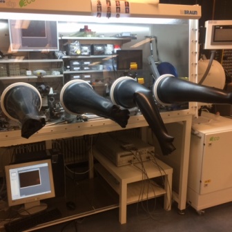
- MBraun glove boxes with N2 environment for electrical measurements of Organic Solar Cells characteristics
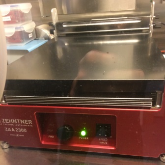
- Zehntner ZAA 2300 automatic film applicator with a kniveblade; adjustable speed, heated surface, adjustable knife height
- Probe station for measurements of Organic Solar Cells characteristics
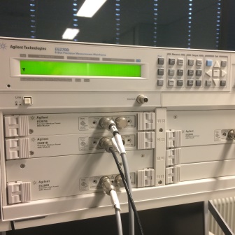
- Agilent E5262A, E5270B & Keithley 4200-SCS IV Analyzers / Semiconductor Characterization Systems
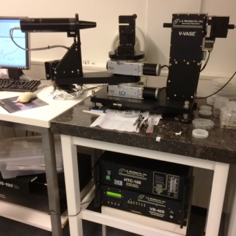
- Ellipsometer J.A. Wollam V-Vase VB-400 for determining thickness and optical properties of thin films
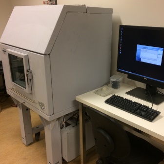
- Bruker Dimension Icon AFM (samples up to 6"), atomic resolution, Scanassist, Peakforce tapping, electrical modes
- Homemade optical setup to determine the EQE of a solar cell
- Photoinduced absorption (PIA) spectroscopy set-up: self-built quasi-steady state photoinduced absorption set-up based on the chopper wheel technique. Several different diode lasers can be used for excitation and a spectral range from the visible to NIR can be covered. The set-up is compatible with a liquid helium cryostat.
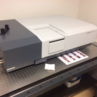
- Shimadzu UV-3600
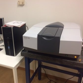
- Shimadzu IRTracer-100
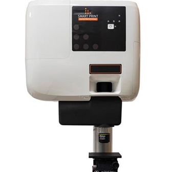
- Maskless Lithography system from Smart Force Technologies (now Microlight3D), Field-Of-View 25.6 mm x 14.4 mm, XY motorized stage, resolution down to 2 μm
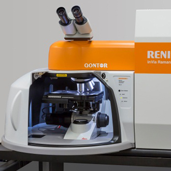
- Renishaw confocal Raman in Via Qontor (includes 2 lasers emitting @ 532 and 786 nm, goes down to 10 cm-1),
| Last modified: | 10 September 2020 1.45 p.m. |